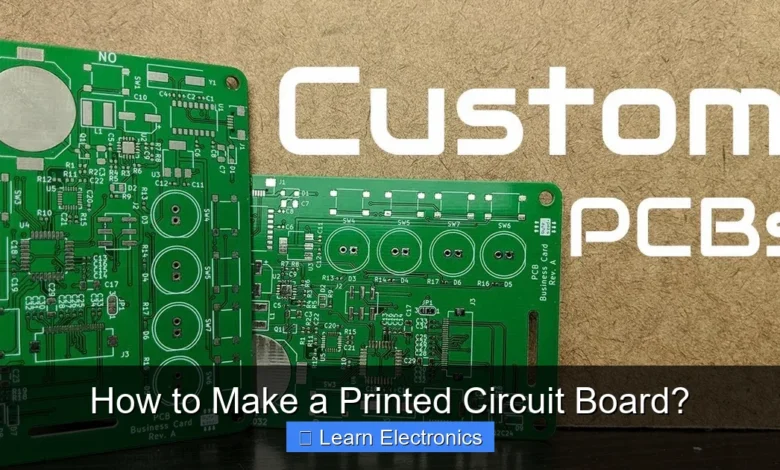
How to Make a Printed Circuit Board? involves transforming a digital circuit design into a physical board with conductive pathways, typically through etching copper from a substrate. This foundational technique is essential for bringing electronic projects to life, providing a robust and compact platform for components. The practice of crafting these boards empowers hobbyists and engineers alike to prototype and build custom electronics with precision and reliability.
Mastering this approach opens up a world of possibilities for custom electronics. From simple sensor modules to complex microcontrollers, understanding the fabrication process behind these vital components is a valuable skill in the world of electronics.
Quick Answers to Common Questions
What’s the easiest way to make a Printed Circuit Board at home?
The toner transfer method is super popular for DIY enthusiasts! You print your circuit design, transfer the toner to a copper board using heat, and then etch away the unwanted copper to reveal your traces.
What essential materials do I need to start making my own PCBs?
You’ll definitely need a copper-clad board, an etchant like ferric chloride, a laser printer, glossy paper for toner transfer, and crucial safety gear like gloves and eye protection.
Is making a Printed Circuit Board at home really worth the effort compared to ordering?
Absolutely! While ordering is convenient for complex designs, DIY PCB making is fantastic for learning the process, rapid prototyping small projects, and getting a deeper understanding of electronics firsthand.
📑 Table of Contents
- Understanding the Basics of Printed Circuit Boards
- Designing Your Circuit Board Layout
- Essential Tools and Materials for PCB Fabrication
- Fabrication Methods: How to Make a Printed Circuit Board at Home
- Etching, Drilling, and Finishing Your PCB
- Assembling and Testing Your Custom PCB
- Etching Solution Comparison Table
- Conclusion
Understanding the Basics of Printed Circuit Boards
Before diving into the fabrication process, it’s crucial to understand what a printed circuit board (PCB) is and its fundamental components. A PCB serves as the foundational structure for most electronic devices, providing mechanical support and electrical connections for electronic components.
The core of a PCB is a non-conductive substrate, typically fiberglass (FR-4), laminated with a thin layer of copper. This copper layer is selectively removed to create the conductive traces, pads, and planes that connect components. Other layers typically include:
- Solder Mask: A protective polymer layer, usually green, that insulates traces from shorting and prevents solder bridges during assembly.
- Silkscreen: A layer for human-readable information, such as component designators, logos, and polarity indicators, printed on top of the solder mask.
PCBs come in various configurations:
- Single-Sided PCBs: Have a copper layer on only one side. Simplest and most cost-effective, suitable for basic circuits.
- Double-Sided PCBs: Feature copper layers on both sides, with plated through-holes (PTHs) connecting traces between layers. Offers higher component density and more complex routing.
- Multi-Layer PCBs: Consist of more than two copper layers separated by insulating material. Used for highly complex and dense circuits, common in modern electronics.
Designing Your Circuit Board Layout
The journey to creating a custom circuit board begins with a well-defined design. This phase translates your circuit schematic into a physical layout that can be manufactured.
Schematic Capture
First, you’ll need to create a schematic, which is a diagram representing your electronic circuit using standard symbols for components and their connections. This is typically done using Electronic Design Automation (EDA) software.
- Software Choices: Popular free and open-source options include KiCad and Fritzing. Commercial software like Eagle (Autodesk Fusion 360) and Altium Designer also offer robust features.
- Component Libraries: Ensure your chosen software has accurate component libraries or the ability to create custom footprints for unique parts.
Layout Design and Routing
Once the schematic is complete, you’ll transition to the layout editor. Here, you’ll place virtual representations of your components (footprints) onto a board outline and then “route” the connections, drawing the copper traces that will physically connect them.
- Component Placement: Strategic placement is critical for performance and manufacturability. Keep related components close, consider heat dissipation, and optimize for shorter trace lengths.
- Routing Traces: Draw the copper paths that connect component pads. Follow design rules to ensure proper spacing between traces, trace width for current capacity, and avoid sharp angles. For double-sided boards, use vias (plated through-holes) to switch traces between layers.
- Ground and Power Planes: Utilize large copper areas (planes) for ground and power connections to improve signal integrity and reduce noise.
- Design Rule Check (DRC): All EDA software includes a DRC tool. Run this frequently to catch errors like short circuits, open circuits, and spacing violations before fabrication.
Generating Fabrication Files
After finalizing your layout and passing all DRC checks, you’ll generate the manufacturing files. The industry standard is Gerber files, which describe each layer of your PCB (copper traces, solder mask, silkscreen). You’ll also generate an NC drill file for the drilling machine.
Essential Tools and Materials for PCB Fabrication
To successfully fabricate a circuit board at home, you’ll need a collection of specific tools and materials. The exact list may vary slightly depending on the method you choose (toner transfer vs. photoresist), but the core items remain similar.
Copper-Clad Laminate
- FR-4 Board: This is the most common substrate, usually available in single-sided or double-sided variants with various copper thicknesses (e.g., 1 oz, 2 oz).
Imaging/Transfer Materials
- For Toner Transfer Method:
- Laser Printer: An essential for printing your design onto special transfer paper. Inkjet printers are not suitable as the toner (plastic particles) is what gets transferred.
- Glossy Paper/Photo Paper: Specific types of glossy paper or magazine pages work best for releasing the toner cleanly. Dedicated toner transfer paper is also available.
- Clothes Iron or Laminator: Used to apply heat and pressure to transfer the toner from the paper to the copper.
- For Photoresist Method:
- Photoresist Film or Spray: A light-sensitive material applied to the copper surface. Dry film photoresist (DFR) is common for hobbyists.
- UV Exposure Unit: A light source (e.g., UV lamp, blacklight, direct sunlight) used to expose the photoresist through a printed transparency.
- Transparency Film: A clear film printed with your PCB design (black areas block UV, clear areas allow it through).
- Developer Solution: Chemical specific to your photoresist type (e.g., sodium carbonate for DFR) to remove unexposed/exposed photoresist.
Etching Supplies
- Etchant: The chemical solution that removes unwanted copper. Common options include:
- Ferric Chloride (FeCl3): A widely used, effective etchant. It is brown, stains easily, and requires careful handling.
- Ammonium Persulfate ((NH4)2S2O8): Clearer, less messy than ferric chloride, often used with a heater to speed up etching.
- Sodium Persulfate (Na2S2O8): Similar to ammonium persulfate, often preferred for its slightly longer shelf life.
- Etching Tank/Tray: A non-metallic, acid-resistant container (plastic, glass) for the etchant. Agitation (e.g., air pump, manual rocking) helps speed up the process.
Drilling and Finishing
- Drill Press or Dremel: For drilling holes for component leads and vias. A dedicated mini drill press offers better precision than hand-held drills.
- Carbide Drill Bits: Small, sharp bits suitable for drilling fiberglass. Various sizes are needed (e.g., 0.8mm for small component leads, 1.0mm for larger ones).
- Steel Wool/Scotch-Brite Pad: For cleaning the copper surface before and after etching.
- Acetone/Thinner: To remove toner (after etching) or photoresist residue.
Safety Gear (CRITICAL!)
- Safety Glasses/Goggles: Protect eyes from chemical splashes.
- Chemical-Resistant Gloves: Nitrile or neoprene gloves are essential to protect skin from etchants and developers.
- Ventilation: Work in a well-ventilated area or outdoors to avoid inhaling chemical fumes.
- Apron/Old Clothes: To protect clothing from stains and splashes.
Fabrication Methods: How to Make a Printed Circuit Board at Home
Once your design is ready and you have your materials, it’s time to bring your custom circuit board to life. Here are the two most common DIY methods:
1. Toner Transfer Method
This simple and popular method uses a laser printer to transfer your circuit design to the copper board.
- Print the Design: Print your mirrored PCB design (top layer viewed from the top, bottom layer viewed from the bottom) onto glossy paper using a laser printer. Ensure black areas are solid toner.
- Prepare the Board: Thoroughly clean the copper-clad board with steel wool or an abrasive pad, then degrease it with rubbing alcohol or acetone. This ensures good toner adhesion.
- Transfer the Toner: Place the printed paper toner-side down onto the clean copper. Apply heat and pressure with a hot clothes iron (no steam) or a laminator. Evenly move the iron over the paper for several minutes, pressing firmly. The heat melts the toner, and the pressure transfers it to the copper.
- Cool and Peel: Allow the board to cool completely. Submerge the board in warm water for 5-10 minutes. The paper will soften, allowing you to gently peel it away, leaving the toner design stuck to the copper. Use a soft brush or your finger to remove any remaining paper pulp, being careful not to scratch the toner.
- Touch-Up (Optional): Inspect the transferred design for any breaks in traces or missing pads. Use a fine-tip permanent marker or a resist pen to fill in gaps.
2. Photoresist Method
This method offers higher precision, especially for finer traces, by using light-sensitive chemicals.
- Apply Photoresist: If using spray photoresist, apply a thin, even coat in a dark room. If using dry film photoresist, carefully laminate it onto the clean copper board using a laminator or rollers, avoiding bubbles.
- Create Transparency Mask: Print your mirrored PCB design onto a transparent film using a laser or inkjet printer. Ensure opaque areas are perfectly black.
- Exposure: Place the transparency mask (ink side down) directly onto the photoresist-coated board. Expose the board to UV light for the recommended time (this varies greatly with your UV source and photoresist type – experimentation is key). The UV light hardens the exposed photoresist, while the unexposed areas remain soluble.
- Develop the Board: Immerse the exposed board in the developer solution (e.g., sodium carbonate for DFR) for a few minutes, gently agitating. The unexposed (softened) photoresist will dissolve, revealing the copper traces that will be etched away. The exposed (hardened) photoresist will remain, protecting the desired copper traces.
- Rinse and Dry: Rinse the developed board thoroughly with water and allow it to dry. Inspect the design for clarity and touch up if necessary.
Etching, Drilling, and Finishing Your PCB
After the design is successfully transferred or developed, the next steps involve removing the unwanted copper and preparing the board for components.
Etching the Copper
This is where the magic happens – the unwanted copper is dissolved, leaving only your circuit traces.
- Prepare the Etchant: Pour your chosen etchant (ferric chloride, ammonium persulfate, etc.) into a non-metallic tray or etching tank. Warm etchants (e.g., 40-50°C) work faster, but be cautious and ensure good ventilation.
- Etch the Board: Carefully place the board into the etchant, ensuring it’s fully submerged. Gently agitate the tray or use an air pump to circulate the etchant, which speeds up the process and ensures even etching. Observe the copper carefully; it will slowly disappear from the exposed areas.
- Monitor and Rinse: Etching time can range from 5 to 30 minutes depending on the etchant, temperature, and agitation. Once all exposed copper is gone, remove the board promptly to prevent under-etching your traces. Rinse the board thoroughly under running water.
- Dispose of Etchant: DO NOT pour used etchant down the drain. It contains dissolved copper and other chemicals. Research local regulations for proper disposal; often, it needs to be neutralized or taken to a hazardous waste facility.
Removing the Resist and Drilling
- Remove Resist: After etching, the toner or hardened photoresist must be removed. Acetone or lacquer thinner works for toner. Specific strippers or strong alkaline solutions are used for photoresist. Scrub gently with a non-abrasive pad.
- Clean the Board: Thoroughly clean the exposed copper with a fine abrasive pad (like Scotch-Brite) to ensure good solder adhesion.
- Drill Holes: Using a drill press or Dremel with appropriate carbide drill bits, carefully drill all component holes and vias. Refer to your PCB design software for the exact drill sizes and locations. Always wear safety glasses when drilling.
Optional Finishing Touches
- Tinning: To prevent oxidation and improve solderability, you can “tin” the copper traces using an immersion tinning solution or by manually flowing solder onto the pads.
- Solder Mask: For professional results, you can apply a DIY solder mask (UV-curable liquid photo solder mask) and expose it, similar to the photoresist method, leaving only the pads exposed for soldering.
- Silkscreen: For component labels, you can apply a silkscreen layer using a toner transfer method or screen printing.
Assembling and Testing Your Custom PCB
With your custom circuit board physically complete, the final steps involve populating it with components and verifying its functionality.
Component Assembly (Soldering)
- Gather Components: Have all your electronic components ready, organized, and identified.
- Placement: Refer to your schematic and layout. Start by placing the smallest components (resistors, diodes) first, then progressively larger ones (IC sockets, capacitors, connectors). Pay close attention to polarity for components like diodes, LEDs, and electrolytic capacitors.
- Soldering: Using a soldering iron and solder, carefully connect each component lead to its corresponding pad on the PCB. Ensure clean, shiny solder joints with good wetting. Avoid cold joints or solder bridges.
Testing and Troubleshooting
After all components are soldered, it’s crucial to test your board before applying power to prevent damage.
- Visual Inspection: Carefully examine the board for any obvious errors:
- Solder Bridges: Unintended connections between adjacent traces or pads.
- Cold Joints: Dull, lumpy solder joints that indicate poor electrical connection.
- Missing Components or Incorrect Polarity: Double-check component placement.
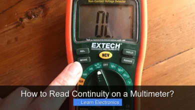
- Continuity Check: Use a multimeter in continuity mode to check for unintended shorts between power and ground lines, or between adjacent traces. Also, verify that all intended connections have continuity.
- Power-Up Test: Apply power carefully. If possible, use a current-limited power supply or a “smoke tester” circuit (like a series light bulb) to prevent damage in case of a short. Monitor current draw and check for any immediate heating or smoke.
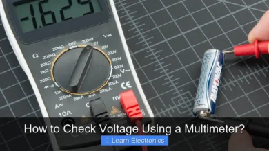
- Functional Testing: Once power is confirmed stable, perform functional tests specific to your circuit. Measure voltages, check signal paths, and verify output as expected.
Common Issues and Debugging
- Open Circuits: A break in a trace or a poor solder joint preventing current flow. Check continuity.
- Short Circuits: Unintended connection between two points that should be separate, often due to solder bridges or etching defects.
- Incorrect Component: Wrong value resistor, capacitor, or reversed polarity for diodes/IC’s.
- Poor Etching: Under-etched traces can lead to shorts; over-etched traces can become too thin or break.
Debugging a custom circuit board requires patience and systematic checking. Start with power and ground, then trace signals step-by-step.
Etching Solution Comparison Table
Choosing the right etchant is important for safety, speed, and environmental impact. Here’s a brief comparison of common DIY options:
| Etchant Type | Pros | Cons | Safety Notes |
|---|---|---|---|
| Ferric Chloride (FeCl3) | Fast, widely available, low cost. | Stains everything, corrosive, difficult disposal, dark solution. | Highly corrosive. Use gloves, eye protection, ventilation. Avoid skin/clothing contact. |
| Ammonium Persulfate | Clear solution (easy to observe), less staining than FeCl3, relatively fast (especially heated). | Slightly more expensive, shorter shelf life, generates fumes. | Corrosive. Use gloves, eye protection, good ventilation. Avoid inhalation of fumes. |
| Sodium Persulfate | Similar to Ammonium Persulfate, clearer, longer shelf life. | Requires heating for optimal speed, similar cost to ammonium persulfate. | Corrosive. Use gloves, eye protection, good ventilation. |
Always consult the Material Safety Data Sheet (MSDS) for any chemical you handle and follow all recommended safety precautions.
Conclusion
Creating your own printed circuit boards is a rewarding endeavor that bridges the gap between theoretical circuit design and tangible electronic devices. While it requires attention to detail, patience, and adherence to safety protocols, the satisfaction of powering up a custom-made board is immense. By understanding the design process, choosing the right fabrication method, and meticulously executing each step from etching to testing, you can transform your electronic ideas into functional realities.
Embrace the learning curve, experiment with different techniques, and remember that practice makes perfect. With each board you create, you’ll gain valuable experience and develop the skills necessary to tackle increasingly complex electronic projects.
Frequently Asked Questions
What essential tools and materials do I need to make a Printed Circuit Board at home?
You’ll primarily need design software (like KiCad or Eagle), a copper-clad board, photoresist film or a toner transfer method, and an etchant solution such as ferric chloride. Basic tools like a UV light source (if using photoresist), a drill, safety gear, and a well-ventilated area are also crucial for successful home fabrication of a Printed Circuit Board.
What are the main steps involved in creating a custom Printed Circuit Board?
The process typically begins with designing your circuit using CAD software, then transferring this design onto a copper-clad board, often using photo-etching or a toner transfer method. Next, the unwanted copper is chemically removed with an etchant, leaving only your circuit traces, followed by drilling holes for component leads and mounting.
What software is commonly used to design a Printed Circuit Board layout?
Popular choices for designing a Printed Circuit Board layout include free, open-source options like KiCad and commercial software such as Eagle (now integrated into Autodesk Fusion 360) and Altium Designer. These powerful tools enable users to create schematics, lay out the board, and generate fabrication files for manufacturing their Printed Circuit Board.
Is making a Printed Circuit Board difficult for a beginner, and what’s a good starting point?
While making your first Printed Circuit Board can seem challenging, many resources and beginner-friendly methods exist to simplify the process. Starting with a simple single-sided board and using a toner transfer method or a basic photo-etching kit can provide a rewarding learning experience for hobbyists, allowing them to gradually master the intricacies of creating a Printed Circuit Board.
As an Amazon Associate, I earn commission from qualifying purchases.