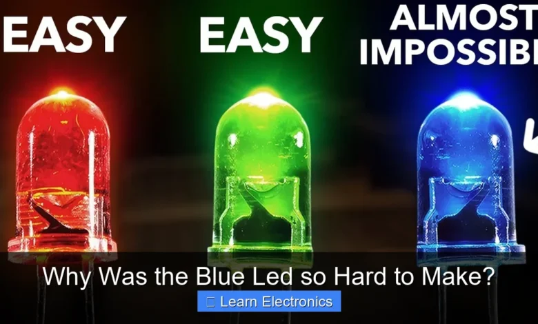
Why Was the Blue LED so Hard to Make? The primary difficulty lay in the extreme material science challenges associated with Gallium Nitride (GaN), the semiconductor compound required for blue light emission. Developing a reliable, efficient p-n junction with this stubborn material proved to be a formidable, multi-decade scientific hurdle. The quest for this elusive component significantly advanced semiconductor physics and engineering.
This approach to creating short-wavelength light from semiconductors faced issues ranging from crystal growth to doping and structural integrity. Researchers spent decades grappling with these fundamental problems, ultimately leading to a breakthrough that revolutionized lighting technology.
Quick Answers to Common Questions
Why was the blue LED so much harder to create than red or green ones?
The main hurdle for the blue LED was finding a semiconductor material that could efficiently emit light in the high-energy blue part of the spectrum. Existing materials worked for red and green, but blue required a special class of materials called wide bandgap semiconductors.
What material finally made the blue LED possible?
The game-changing material was Gallium Nitride (GaN), a wide bandgap semiconductor that allowed for efficient light emission in the blue and ultraviolet range. It took incredible ingenuity to grow high-quality GaN crystals and make them work reliably.
Why was creating a blue LED such a monumental achievement?
The invention of the blue LED completed the RGB color trifecta, which meant we could finally create true-color displays and, most importantly, incredibly efficient white LED lighting. This innovation fundamentally transformed how we light our world, saving immense amounts of energy.
📑 Table of Contents
- The Material Science Conundrum: Gallium Nitride (GaN)
- The Quest for Quality: Substrates and Lattice Mismatch
- Manufacturing Hurdles and Epitaxial Growth: Why Was the Blue LED so Hard to Make?
- The Physics Behind Blue Light Emission
- The Human Element: Perseverance and Innovation in Making Blue LEDs
- Impact and Legacy: The Dawn of White LEDs and Beyond
- Conclusion
The Material Science Conundrum: Gallium Nitride (GaN)
Unlike its red and green counterparts, which relied on relatively well-understood materials like Gallium Arsenide (GaAs) and Gallium Phosphide (GaP), the blue LED demanded a semiconductor with a significantly larger band gap. This property dictates the energy of the photons emitted, and for blue light, that energy is higher, requiring a wider band gap material. Gallium Nitride (GaN) emerged as the theoretical candidate, but its practical implementation was fraught with difficulties.
The Problem with Growing GaN Crystals
One of the foundational challenges was growing high-quality GaN crystals. Unlike silicon or gallium arsenide, which could be grown into large, pure single crystals, GaN proved extremely difficult to crystallize. It has a high melting point and decomposes before melting at atmospheric pressure, making traditional melt-growth techniques impossible. Researchers had to resort to vapor-phase deposition methods, growing thin films of GaN on foreign substrates.
The resulting material often suffered from a high density of defects, dislocations, and impurities. These imperfections dramatically reduced the efficiency of the LED, acting as traps for electrons and holes, preventing them from recombining to emit light. Imagine trying to build a perfectly straight wall with uneven, cracked bricks; the structural integrity, and thus the efficiency of the LED, would be severely compromised.
Doping Difficulties for P-type Material
For any semiconductor device, including an LED, to work, it needs both n-type (electron-rich) and p-type (hole-rich) regions to form a p-n junction. While n-type GaN could be relatively easily created by doping with silicon, making stable and efficient p-type GaN was a monumental obstacle. Magnesium was identified as the ideal dopant for p-type GaN, but it didn’t behave as expected.
Early attempts at magnesium doping resulted in highly resistive material that barely conducted electricity, effectively preventing the formation of a functional p-n junction. It was later discovered by Isamu Akasaki and Hiroshi Amano that a post-growth annealing step in a nitrogen atmosphere, or electron beam irradiation, was necessary to activate the magnesium dopants by removing hydrogen atoms that passivated them. This discovery was a pivotal moment, finally enabling the creation of viable p-type GaN and making the p-n junction a reality for blue light emission.
The Quest for Quality: Substrates and Lattice Mismatch
Since large GaN single crystals couldn’t be grown, scientists had to grow thin films on other materials, known as substrates. The choice of substrate was critical, as it directly impacted the quality and performance of the epitaxial GaN layer.
Sapphire: A Double-Edged Sword
Sapphire (Al2O3) emerged as the most common substrate due to its high thermal stability, transparency, and availability. However, it presented significant problems. The crystalline structure of sapphire is vastly different from that of GaN, leading to a substantial “lattice mismatch.” This refers to the difference in the spacing of atoms in the crystal lattices of the two materials. When GaN was grown on sapphire, this mismatch created immense strain, leading to a high density of crystalline defects, known as dislocations, in the GaN layer.
Furthermore, sapphire is an electrical insulator, meaning it does not conduct electricity. This required complex device designs where both electrical contacts had to be made on the top surface of the GaN layer, adding to manufacturing complexity and potentially reducing light extraction efficiency.
Overcoming Lattice Dislocation
To mitigate the lattice mismatch, researchers developed various techniques. One crucial innovation was the use of a low-temperature GaN buffer layer. By depositing a very thin layer of GaN at a lower temperature before growing the main high-temperature GaN layer, the strain could be gradually relaxed, significantly reducing the density of defects. This approach, pioneered by Akasaki and later improved by Shuji Nakamura, was instrumental in achieving GaN layers of sufficient quality for functional devices.
Manufacturing Hurdles and Epitaxial Growth: Why Was the Blue LED so Hard to Make?
The highly specialized techniques required for growing GaN layers represented significant manufacturing hurdles. The precise control over temperature, gas flow, and pressure needed for epitaxial growth pushed the boundaries of existing equipment and processes.
Metalorganic Chemical Vapor Deposition (MOCVD)
Metalorganic Chemical Vapor Deposition (MOCVD) became the dominant technique for growing GaN films. In MOCVD, metalorganic precursors (like trimethylgallium for gallium and ammonia for nitrogen) are introduced into a reaction chamber at high temperatures, where they decompose and react to deposit a thin film of GaN onto the substrate. This process requires extremely high purity gases and precise control over gas flow rates and temperature profiles (often exceeding 1000°C).
The design and operation of MOCVD reactors are incredibly complex. Maintaining uniform temperature and gas flow across a large wafer area is challenging, directly impacting the uniformity and quality of the GaN film. This made scaling up production difficult and expensive in the early days.
The High Costs and Complexities of the Process
The equipment for MOCVD is expensive, and the process itself is time-consuming. Growing a single high-quality GaN wafer could take many hours, sometimes even days, with each step requiring meticulous calibration and monitoring. The precursors used are often toxic and pyrophoric (spontaneously igniting in air), necessitating stringent safety protocols and specialized handling equipment. These factors contributed significantly to the high initial cost of blue LEDs and the complexity of their manufacture.
The Physics Behind Blue Light Emission
Understanding the fundamental physics of light emission helps to clarify why blue was so elusive compared to other colors. It all boils down to band gap energy and wavelength.
Band Gap Energy and Wavelengths
In a semiconductor, electrons reside in specific energy bands. When an electron drops from a higher energy level (conduction band) to a lower energy level (valence band), it releases energy. In an LED, this energy is released as a photon of light. The energy difference between these two bands is called the “band gap energy.”
The color of the emitted light is inversely proportional to its wavelength, which in turn is directly related to the band gap energy. Blue light has a shorter wavelength than red or green light, meaning it requires a higher energy photon, and thus a wider band gap semiconductor material. Red LEDs, using materials like GaAsP, have smaller band gaps, making them relatively easier to produce with existing material science techniques.
Why Red and Green were Easier
Red and green LEDs were developed much earlier because their required band gap energies could be achieved with materials that were far easier to grow and dope effectively. Materials like Gallium Arsenide (GaAs) and Gallium Phosphide (GaP) allowed for crystal growth with fewer defects and simpler doping processes to create the necessary p-n junctions. The material science for these compounds was mature, having been extensively studied for other semiconductor applications, making the leap to red and green light emitters less daunting than the entirely new territory of GaN for blue light.
The Human Element: Perseverance and Innovation in Making Blue LEDs
Beyond the scientific and engineering hurdles, the success of the blue LED is a testament to extraordinary human perseverance. Many research groups worldwide pursued this goal, often facing skepticism and limited funding due to the perceived difficulty.
Key Researchers and Their Contributions
Several individuals played critical roles, leading to the Nobel Prize in Physics in 2014 for Isamu Akasaki, Hiroshi Amano, and Shuji Nakamura. Akasaki and Amano, working at Nagoya University, made fundamental breakthroughs in growing high-quality GaN films on sapphire using a low-temperature buffer layer and later achieved the first efficient p-type GaN. Nakamura, working at the small Japanese company Nichia Corporation, independently developed his own high-brightness blue LED using similar techniques, demonstrating its commercial viability and pushing the boundaries of efficiency.
The Unconventional Path to Success
The research path for blue LEDs was often unconventional. Nakamura, for instance, worked largely in isolation from the broader academic community, driven by Nichia’s singular focus on commercializing the technology. His relentless experimentation, sometimes against internal company advice, led to rapid progress. The willingness to tackle seemingly insurmountable problems, and to try novel approaches when conventional methods failed, was a hallmark of this groundbreaking research.
Impact and Legacy: The Dawn of White LEDs and Beyond
The successful development of the blue LED wasn’t just about illuminating a new color; it was the missing piece that unlocked a revolution in lighting and display technology.
The White Light Revolution
With blue LEDs, scientists finally had the three primary colors of light (red, green, blue) necessary to create white light. There are two main ways this is achieved:
- RGB Mixing: Combining individual red, green, and blue LEDs in a single package. This offers precise color control and is common in displays.
- Phosphor Conversion: This is the more common method for general illumination. A blue LED is coated with a yellow phosphor material. The blue light excites the phosphor, causing it to emit yellow light. When the emitted yellow light mixes with some of the unabsorbed blue light, it appears white to the human eye. This method is highly efficient and simpler to manufacture for many applications.
This capability allowed for the creation of energy-efficient, long-lasting white light sources, replacing traditional incandescent and fluorescent bulbs and leading to enormous energy savings globally.
Energy Efficiency and Global Impact
The blue LED’s breakthrough ushered in the era of LED lighting, which is significantly more energy-efficient than previous technologies. A typical LED bulb consumes 75-80% less energy than an incandescent bulb and lasts up to 25 times longer. This reduction in electricity consumption has profound environmental and economic benefits, lowering carbon emissions and reducing energy bills for consumers and businesses worldwide. From smartphone screens and large-screen TVs to traffic lights and general illumination, the impact of overcoming the initial challenges for this technology is truly pervasive.
LED Material and Color Characteristics
To further illustrate the differences, here’s a brief overview of common LED materials and their associated colors:
| LED Color | Primary Material | Approx. Wavelength (nm) | Relative Band Gap Energy | Historical Difficulty |
|---|---|---|---|---|
| Red | Gallium Arsenide Phosphide (GaAsP) / Aluminum Gallium Indium Phosphide (AlGaInP) | 620-650 | Lower | Easier (earliest developed) |
| Orange/Yellow | Gallium Arsenide Phosphide (GaAsP) / Aluminum Gallium Indium Phosphide (AlGaInP) | 585-610 | Medium-Lower | Moderate |
| Green | Gallium Phosphide (GaP) / Aluminum Gallium Indium Phosphide (AlGaInP) | 520-550 | Medium | Moderate (earlier than blue) |
| Blue | Gallium Nitride (GaN) / Indium Gallium Nitride (InGaN) | 450-480 | High | Extremely Difficult (breakthrough in 1990s) |
| White | Blue LED + Yellow Phosphor | Broad Spectrum | N/A (conversion) | Dependent on Blue LED |
Conclusion
The journey to develop the blue LED was a challenging odyssey through advanced material science, crystal growth complexities, and semiconductor physics. It required overcoming fundamental hurdles in growing high-quality Gallium Nitride crystals, effectively doping them to create p-type material, and managing the profound lattice mismatch with suitable substrates. The scientific and engineering community spent decades grappling with these issues, often with limited success and facing considerable skepticism.
Ultimately, the perseverance of dedicated researchers like Akasaki, Amano, and Nakamura led to the breakthroughs that made stable and efficient blue light-emitting diodes a reality. This accomplishment not only filled the missing link in the color spectrum, enabling true white LED lighting, but also ignited a revolution in energy efficiency and display technology that continues to shape our modern world. The story of its development stands as a powerful testament to the impact of fundamental research and unwavering dedication in the face of daunting scientific challenges.
Frequently Asked Questions
Why was the blue LED so difficult to create compared to other colors?
Red and green LEDs could be made with existing semiconductor materials like gallium arsenide and gallium phosphide, which were well understood. However, producing blue light requires a material with a much wider energy bandgap, which was incredibly challenging to grow and work with efficiently without introducing fatal defects. This fundamental material difference was the core difficulty in developing the blue LED.
What were the main material science problems with making the blue LED?
The primary challenge for the blue LED was finding and effectively utilizing a suitable semiconductor material, specifically gallium nitride (GaN). It was exceedingly difficult to grow high-quality GaN crystals on existing substrates without introducing many defects, and crucial techniques for “doping” it to create both p-type and n-type layers were initially elusive. These material science hurdles severely hindered its development for decades.
How did the challenges in crystal growth affect the development of the blue LED?
Growing high-quality gallium nitride (GaN) crystals was a significant hurdle because there was no suitable substrate that matched GaN’s crystal lattice structure and thermal expansion well. This led to many dislocations and defects in the grown material, which drastically reduced the efficiency and lifespan of early blue LEDs. Overcoming these growth issues was crucial for practical devices.
Who were the key researchers involved in finally making the blue LED practical?
The breakthrough was largely attributed to three Japanese scientists: Isamu Akasaki, Hiroshi Amano, and Shuji Nakamura, who shared the Nobel Prize in Physics in 2014 for their work. Their independent and collaborative efforts, particularly in developing high-quality gallium nitride (GaN) crystals and effective p-type doping, led to the development of efficient blue light-emitting diodes. Their persistence revolutionized lighting technology.
What major innovations did the invention of the blue LED enable?
The creation of the efficient blue LED completed the RGB (red, green, blue) color spectrum, making it possible to produce energy-efficient white light by combining it with red and green LEDs or by using a phosphor coating. This paved the way for modern LED lighting, full-color LED displays, smartphones, and countless other technological advancements that rely on efficient solid-state illumination.
As an Amazon Associate, I earn commission from qualifying purchases.