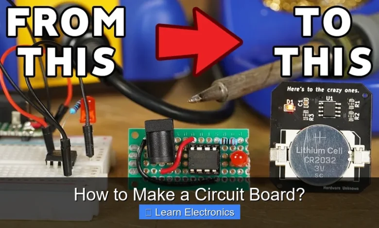
How to Make a Circuit Board? This fundamental skill in electronics involves a series of precise steps, transforming a digital design into a tangible, functional electronic component. Mastering this method allows for the creation of custom circuitry tailored to specific project needs, offering immense flexibility for hobbyists and professionals alike.
Quick Answers to Common Questions
What’s the very first step when you want to make a circuit board?
Before you even think about etching, the crucial first step is to design your circuit and lay out its components using a PCB design software. This digital blueprint is essential to truly understand how to make a circuit board successfully.
Do I need expensive equipment to learn how to make a circuit board at home?
Not at all for basic projects! You can start with relatively inexpensive tools like a photo-etching kit, a laser printer, and chemicals such as ferric chloride or ammonium persulfate to get started with making your own circuit board.
Why would I bother making my own circuit board instead of buying one?
Learning how to make a circuit board offers incredible customization, allows for rapid prototyping of unique designs, and is a fantastic way to deepen your understanding of electronics from the ground up! It’s a truly rewarding skill for any maker.
📑 Table of Contents
Understanding Circuit Boards and Their Fundamentals
Before diving into the practical steps, it’s essential to grasp what a circuit board is and why it’s so critical in modern electronics. A Printed Circuit Board (PCB) serves as the foundational platform for mounting and connecting electronic components, providing mechanical support and electrical connections.
What is a PCB?
A PCB consists of layers of conductive material (typically copper) laminated onto a non-conductive substrate (like fiberglass). The copper traces etched onto these layers create pathways for electrical current, connecting various components in a predefined arrangement. This intricate design ensures reliable and efficient operation of electronic devices, from simple gadgets to complex computer systems.
Essential PCB Components
While the PCB itself is a component, it also hosts a myriad of others. Key components include:
- Substrate: The insulating material that forms the body of the board. Common types include FR-4 (fiberglass-reinforced epoxy).
- Copper Traces: The conductive pathways for electrical signals.
- Solder Mask: A protective layer, usually green, applied over the copper traces to prevent short circuits during soldering and protect against environmental damage.
- Silkscreen: A layer for printing labels, component designators, and symbols, aiding in assembly and troubleshooting.
- Pads: Copper areas where components are soldered.
- Vias: Plated holes that connect traces between different layers of a multi-layer board.
Design Phase: From Concept to Digital Blueprint
The journey of circuit board creation begins long before any physical material is handled. It starts with a comprehensive design phase, utilizing specialized software to translate an electronic concept into a precise digital blueprint.
Schematic Capture
The first step in the design process is schematic capture. This involves drawing the circuit diagram using Electronic Design Automation (EDA) software. Here, you select and connect virtual components (resistors, capacitors, microcontrollers, etc.) to define the electrical relationships and functionality of your circuit. It’s a logical representation of the circuit, focusing on connectivity rather than physical layout.
PCB Layout Design
Once the schematic is complete and verified, the next crucial step is PCB layout design. In this phase, the logical connections from the schematic are translated into physical traces on the board. This involves:
- Component Placement: Strategically positioning components on the board to optimize signal integrity, minimize trace lengths, and ensure ease of assembly.
- Routing: Drawing the copper traces that connect the component pads as defined in the schematic. This requires careful consideration of trace width, spacing, and impedance.
- Layer Stack-up: For multi-layer boards, defining the arrangement and properties of each layer (signal, ground, power planes).
Attention to detail in this stage is paramount, as layout decisions directly impact the circuit’s performance, reliability, and manufacturability. Many designers consider this to be the most critical step in the entire process.
Design Rules Check (DRC)
Before moving to fabrication, a thorough Design Rules Check (DRC) is performed. This automated process uses predefined rules (e.g., minimum trace width, minimum spacing between traces, pad-to-trace clearance) to identify any violations in the layout. Catching errors at this stage saves significant time and cost by preventing costly re-spins of the physical board.
Preparing for Fabrication: Materials and Pre-press
With a verified digital design in hand, the next phase focuses on preparing the physical materials and translating the digital blueprint into a format suitable for manufacturing.
Substrate Materials
The choice of substrate material is critical and depends on the application’s requirements for electrical performance, thermal stability, and cost. FR-4 is the most common, offering a good balance of properties. However, for high-frequency or high-power applications, materials like Rogers laminates or ceramic substrates might be used.
Copper Cladding
The substrate typically comes pre-clad with copper foil on one or both sides. The thickness of this copper (measured in ounces per square foot) is chosen based on the current carrying capacity requirements of the traces.
Photo-Tool Generation
The digital layout files are converted into high-resolution photo-tools (films) or direct imaging data. These photo-tools are essentially transparencies, with opaque areas representing copper traces and transparent areas representing where copper will be removed. This is analogous to a negative in traditional photography, used to transfer the pattern onto the copper-clad laminate.
The Fabrication Process: How to Make a Circuit Board?
This is where the magic happens – the physical transformation of raw materials into a functional printed circuit board. This intricate process involves multiple chemical and mechanical steps, each demanding precision.
Drilling and Plating Through-Holes
The process begins with drilling precise holes for component leads (through-hole components) and vias (connections between layers). After drilling, a critical step called electro-less copper deposition is performed, coating the inside of the drilled holes with a thin layer of copper. This makes the holes conductive, enabling electrical connections between different layers. Subsequent electroplating thickens this copper layer to ensure robust connections.
Etching the Copper
The core of creating the traces involves photolithography and etching. A photoresist material is applied to the copper-clad board and exposed to UV light through the photo-tool. The exposed areas of the photoresist either harden or soften depending on whether it’s a positive or negative resist. After development, the unhardened resist is removed, exposing areas of copper. The board is then submerged in an etchant solution (e.g., ferric chloride or ammonium persulfate), which dissolves the exposed copper, leaving behind the desired copper traces protected by the hardened photoresist. Finally, the remaining photoresist is stripped off.
Solder Mask Application
A liquid photoimageable solder mask is applied over the entire board. This mask is then exposed to UV light through another photo-tool, which selectively hardens the mask over the copper traces, leaving the pads exposed for soldering. The unhardened mask is washed away, resulting in the characteristic green (or other colors) protective layer. This layer prevents solder bridges and protects the copper from oxidation and environmental contaminants.
Silkscreen Printing
The final layer applied is the silkscreen, typically in white ink. This layer contains component designators (e.g., R1, C2), polarity indicators, company logos, and other helpful information for assembly, testing, and troubleshooting. It’s usually applied using an inkjet printer or screen printing process.
Surface Finish Application
To prevent oxidation of the exposed copper pads and ensure good solderability, a surface finish is applied. Common finishes include HASL (Hot Air Solder Leveling), ENIG (Electroless Nickel Immersion Gold), OSP (Organic Solderability Preservative), and immersion silver/tin. Each finish offers different benefits regarding cost, shelf life, and suitability for specific soldering processes.
Cutting and Routing
Finally, the individual circuit boards are cut or routed from the larger panel using a CNC router or a V-score machine. This separates the individual PCBs, often leaving small tabs or “mouse bites” that need to be snapped or filed off.
| Step | Description | Primary Purpose |
|---|---|---|
| Design | Schematic & Layout using EDA software. | Define circuit functionality & physical connections. |
| Drilling | Creating holes for components & vias. | Provide component mounting points & inter-layer connectivity. |
| Etching | Removing unwanted copper via chemical process. | Form the conductive traces and pads. |
| Solder Mask | Applying a protective, insulating layer. | Prevent shorts, protect copper, aid soldering. |
| Silkscreen | Printing labels & designators. | Aid assembly, identification, and troubleshooting. |
| Surface Finish | Coating exposed copper pads. | Ensure solderability & prevent oxidation. |
Assembly: Populating Your Circuit Board
After fabrication, the bare PCB is ready to be populated with electronic components. This assembly process transforms the inert board into a live, functional circuit.
Component Sourcing
The first step in assembly is acquiring all the necessary electronic components. This involves sourcing parts from distributors, ensuring correct values, packages (e.g., SMD vs. through-hole), and quantities.
Solder Paste Application
For Surface Mount Technology (SMT) components, solder paste (a mixture of tiny solder balls and flux) is precisely applied to the component pads using a stencil printing machine. This machine aligns a metal stencil with the PCB and forces solder paste through the stencil’s apertures onto the pads.
Pick-and-Place
Automated pick-and-place machines then precisely position surface mount components onto the solder paste-covered pads. These machines are incredibly fast and accurate, handling thousands of components per hour.
Reflow Soldering
Once all SMT components are placed, the board passes through a reflow oven. The oven has several temperature zones that gradually heat the board, melting the solder paste, allowing it to wet the component leads and pads, and form strong electrical and mechanical connections. The board then cools, solidifying the solder joints.
Inspection and Testing
After soldering, boards undergo rigorous inspection and testing. This can include Automated Optical Inspection (AOI) to check for manufacturing defects (missing components, incorrect polarity, solder bridges), X-ray inspection for complex packages, and In-Circuit Testing (ICT) to verify electrical functionality. Finally, functional testing ensures the completed circuit board performs as designed.
Tips for Successful Circuit Board Creation
Creating functional circuit boards consistently requires diligence and adherence to best practices. Here are some tips to help you achieve success in this practice:
Common Pitfalls to Avoid
- Ignoring Design Rules: Always adhere to manufacturer design rules regarding trace width, spacing, and drill sizes.
- Poor Component Placement: Inadequate placement can lead to signal integrity issues, thermal problems, or difficulty in assembly.
- Inadequate Power/Ground Planes: Proper power and ground plane design is crucial for stable operation and EMI reduction.
- Lack of Documentation: Always document your design choices, component lists, and test procedures.
- Not Testing Thoroughly: Relying solely on simulations can be risky; always prototype and test your designs in the real world.
Tools and Software Recommendations
- EDA Software: For design, popular options include Altium Designer (professional), Eagle (hobbyist/mid-range), KiCad (open-source), and EasyEDA (web-based).
- Prototyping Tools: Breadboards and perfboards are excellent for initial concept validation.
- Soldering Equipment: A good quality soldering iron, solder wire, flux, and desoldering tools are essential for assembly and rework.
- Measurement Tools: Multimeter, oscilloscope, and logic analyzer are invaluable for testing and debugging.
Conclusion
The journey of creating a circuit board, from initial concept to a fully functional electronic device, is a multifaceted process demanding precision, knowledge, and patience. While it may seem daunting at first, breaking it down into manageable stages – design, fabrication, and assembly – reveals a logical and rewarding path. By understanding each step, utilizing appropriate tools, and adhering to best practices, you can successfully bring your electronic ideas to life, whether for personal projects or professional applications. The ability to craft custom circuitry is a powerful asset in the world of electronics, opening up endless possibilities for innovation and problem-solving.
Frequently Asked Questions
What materials do I need to make a circuit board?
To make a basic circuit board at home, you’ll typically need a copper-clad board (FR-4 substrate), photoresist film or a permanent marker, an etchant solution (like ferric chloride or ammonium persulfate), and a drill for component holes. You will also need solder, flux, and the electronic components for your specific circuit design.
What are the main steps involved in making a circuit board at home?
The primary steps for making a circuit board involve designing your circuit layout on a computer or by hand, then transferring this design onto the copper-clad board using a method like toner transfer or photoetching. Next, you’ll etch away the unwanted copper, leaving only your circuit traces. Finally, you drill holes for component placement and solder your electronic components onto the board.
Is it difficult to make my own circuit board, and what skills are required?
Making your own circuit board can be challenging initially, requiring patience and attention to detail, but it becomes much easier with practice. Essential skills include understanding basic electronics, being precise with measurements, and careful handling of chemicals for etching. Familiarity with design software is also beneficial for creating accurate layouts.
How can I design a circuit board layout before manufacturing?
You can design a circuit board layout using specialized Electronic Design Automation (EDA) software such as KiCad, Eagle, or Altium Designer. These tools allow you to create schematics, arrange components, and route traces on a virtual board. A well-planned digital design is crucial for ensuring your physical circuit board functions correctly.
As an Amazon Associate, I earn commission from qualifying purchases.