Learning how to make PCB board involves a fascinating journey from a digital design to a tangible electronic circuit. This method, often referred to as PCB prototyping, allows hobbyists and engineers alike to bring their electronic ideas to life with precision and control. Mastering this practice unlocks a world of custom electronics, enabling you to create boards perfectly tailored to your unique projects.
The process, while requiring careful attention to detail, is incredibly rewarding. It typically involves several key stages, from initial design and material preparation to transferring the circuit pattern, etching, and final finishing. Understanding each step ensures a successful outcome and opens up possibilities for more complex and robust designs.
Quick Answers to Common Questions
What’s the very first step in how to make a PCB board?
The journey to make a PCB board always begins with design! You’ll first need to create a schematic diagram and then lay out the traces and components using dedicated PCB design software.
Can I really make a PCB board at home, or do I need a factory?
Absolutely, you can definitely learn how to make a PCB board at home, especially for simpler projects! While professional boards are often factory-made, hobbyists frequently use methods like toner transfer or photoresist etching with basic tools and chemicals.
What software should I use to design my PCB board?
When it comes to designing your PCB board, there are many fantastic software options available! Popular choices range from free tools like KiCad and EasyEDA to professional industry standards like Altium Designer and Eagle, catering to various skill levels and project complexities.
📑 Table of Contents
Designing Your PCB Layout
The very first step in creating any custom printed circuit board is the design phase. This is where your circuit schematic is translated into a physical layout that defines the traces, pads, and component placement on the board. Modern software tools make this process accessible and highly efficient.
Schematic Capture
Before you can lay out the physical board, you need a clear electrical schematic. This diagram illustrates all the components and their interconnections logically. Software like KiCad, Eagle, or Altium Designer allows you to draw your schematic, assigning footprints (the physical representation of a component) to each part. This foundational step ensures that your circuit is electrically sound before you commit to a physical layout.
Board Layout and Routing
Once the schematic is complete, you move to the board layout editor. Here, you define the board’s physical dimensions and arrange your components within those boundaries. Key considerations include minimizing trace lengths, avoiding unnecessary crossovers, and ensuring adequate spacing for signal integrity and manufacturability. Routing involves drawing the copper traces that connect the component pads, following the paths defined in your schematic. This practice can be done manually for optimal control or with auto-routers that automate much of the work.
Design Rule Checks (DRC)
Before finalizing your design, running a Design Rule Check (DRC) is crucial. DRC tools automatically identify potential issues such as short circuits, open circuits, incorrect trace widths, and insufficient spacing between traces or pads. Adhering to these rules is vital for ensuring your PCB will function correctly and can be fabricated without errors. Many design software packages allow you to customize these rules based on your specific manufacturing constraints or desired board quality.
Preparing Your Workspace and Materials
A well-prepared workspace and the right materials are essential for a smooth and successful PCB fabrication process. This stage lays the groundwork for all subsequent steps.
Essential Tools and Supplies
To embark on this technique, you’ll need several key items. These typically include:
- Copper Clad Laminate: The base material, usually FR-4, with a layer of copper on one or both sides.
- Photoresist Film or Spray: A light-sensitive material used to transfer your circuit pattern.
- UV Light Source: For exposing the photoresist (a UV lamp or even direct sunlight can work).
- Developer Solution: To remove unexposed photoresist.
- Etchant: A chemical solution (e.g., Ferric Chloride, Ammonium Persulfate) to dissolve unwanted copper.
- Drill Press and Drill Bits: Small bits (0.5mm to 3mm) for component leads and mounting holes.
- Protective Gear: Gloves, safety glasses, and a well-ventilated area are paramount.
- Artwork Prints: High-resolution printouts of your PCB design on transparent film (e.g., OHP sheets).
Choosing Your Copper Clad Laminate
FR-4 is the most common and cost-effective material for hobbyist PCB making. It’s a fiberglass-reinforced epoxy laminate, available in various thicknesses (e.g., 1.6mm is standard) and copper weights (e.g., 1oz, 2oz). For simple, low-frequency circuits, 1oz copper is generally sufficient. Double-sided laminates are common, allowing for more complex routing and component placement.
Safety First
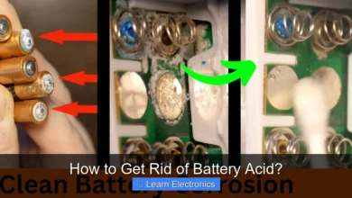
Working with chemicals like etchants and developers requires strict adherence to safety protocols. Always wear appropriate personal protective equipment (PPE), including chemical-resistant gloves and eye protection. Work in a well-ventilated area to avoid inhaling fumes. Have baking soda or another neutralizing agent on hand for spills, especially when using acidic etchants. Proper disposal of chemical waste is also critical to environmental responsibility.
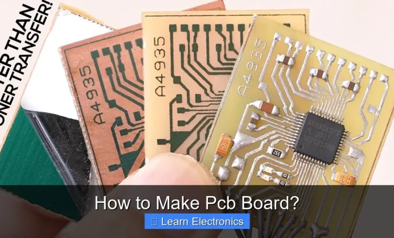
Transferring the Design to Copper
This critical phase involves accurately transferring your circuit layout from the digital design onto the copper surface of the laminate. The photolithography method is widely used for its precision.
Printing the Artwork
Your PCB design needs to be printed onto a transparent film. This artwork serves as a mask during UV exposure. It’s crucial that these prints are high-resolution, dense black, and perfectly scaled. Laser printers on OHP (Overhead Projector) film or specialized photographic films work best. For double-sided boards, ensure precise alignment of the top and bottom layers by printing registration marks on both films.
Applying Photoresist
Before applying photoresist, the copper clad board must be meticulously cleaned. Any grease, dust, or fingerprints can lead to imperfections. Industrial alcohol or abrasive cleaners followed by a thorough rinse and dry are often used. Photoresist can be applied as a dry film, which is laminated onto the copper, or as a liquid spray. Dry film photoresist is generally preferred for hobbyists due to its consistency and ease of application, although it requires a laminator or steady hands with a roller.
UV Exposure and Development
Once the photoresist is applied, the printed artwork is carefully placed over the photoresist layer on the copper board. For negative photoresists (most common), the clear areas of your artwork will allow UV light to pass through, hardening the photoresist underneath. The black areas block the UV light, keeping the photoresist soft. The board is then exposed to UV light for a specific duration, which varies based on the light source and photoresist type. After exposure, the board is submerged in a developer solution, which dissolves the unexposed (soft) photoresist, leaving a hardened resist pattern that mirrors your circuit traces and pads.
How to Make PCB Board? The Etching Process
With the design now transferred as a resist layer, the etching process removes the unwanted copper, revealing your circuit paths. This is perhaps the most visually satisfying stage of the entire fabrication. This approach is fundamental to isolating your circuit.
Preparing the Etchant
Various etchants can be used, each with its own advantages and safety considerations. Ferric Chloride is a common choice, known for its effectiveness, though it can stain. Ammonium Persulfate is another popular option, often preferred for its cleaner results and less aggressive fumes. Regardless of the etchant, it should be prepared according to the manufacturer’s instructions, often requiring heating to an optimal temperature (e.g., 40-50°C for Ferric Chloride) for faster and more consistent etching. Always use a non-metallic container, such as a plastic tray.
The Etching Bath
Carefully submerge the developed PCB into the etchant bath. Gentle agitation (rocking the tray or using an air bubbler) is crucial to ensure fresh etchant continuously contacts the copper, leading to even etching. The etching time will depend on the etchant type, temperature, concentration, and the thickness of the copper. Keep a close eye on the process; you’ll see the exposed copper dissolving, leaving behind the protected traces. Over-etching can lead to undercut traces, while under-etching will leave unwanted copper bridges.
Here’s a comparison of common etchants:
| Etchant Type | Pros | Cons | Safety Notes |
|---|---|---|---|
| Ferric Chloride | Fast, effective, readily available | Stains heavily, corrosive, toxic fumes | Gloves, eye protection, ventilation, avoid contact with skin/clothing |
| Ammonium Persulfate | Cleaner process, less staining, clear solution | Slower than Ferric Chloride, requires heating | Gloves, eye protection, ventilation, avoid contact with skin/clothing |
| Sodium Persulfate | Similar to Ammonium Persulfate, good for fine traces | Similar to Ammonium Persulfate | Gloves, eye protection, ventilation |
Post-Etch Cleaning
Once etching is complete and all unwanted copper is dissolved, remove the board from the etchant and rinse it thoroughly with water to stop the etching process. Then, the remaining photoresist needs to be removed. This can usually be done with a resist stripper solution or by scrubbing with fine steel wool or a chemical like acetone or denatured alcohol. After stripping the resist, clean the board again to remove any residue, leaving shining copper traces.
Drilling and Finishing Your Custom PCB
With the circuit traces now clearly defined, the next stage is to drill the necessary holes and apply any protective coatings to complete your custom PCB.
Precision Drilling
All component leads, vias (connections between layers), and mounting holes need to be drilled. A high-speed drill press with a set of micro-drill bits is ideal for this. Common drill bit sizes range from 0.5mm to 1.5mm for component leads and larger for mounting holes. For double-sided boards, ensuring accurate alignment before drilling is paramount. Start with smaller holes for accuracy and gradually increase size if needed. This step demands a steady hand and attention to detail to prevent breaking bits or damaging traces.
Deburring and Cleaning
After drilling, small burrs of copper or fiberglass may be present around the holes. These should be carefully removed using fine sandpaper, a deburring tool, or a hobby knife to ensure smooth surfaces and prevent any electrical shorts. Following deburring, a final cleaning with industrial alcohol removes any dust or debris, preparing the board for soldering.
Optional: Soldermask and Silkscreen
For a more professional finish and added durability, you can apply a soldermask. This is a thin, protective polymer layer (typically green) that covers the copper traces, preventing solder bridges and protecting against environmental factors. It’s usually applied with a screen printing process or as a UV-curable liquid/film, followed by exposure and development. A silkscreen layer, which provides component designators (e.g., R1, C2) and outlines, can also be applied using a similar screen printing technique, aiding assembly and troubleshooting.
Optional: Tinning for Protection
To prevent oxidation of the exposed copper pads and traces, a layer of tin can be applied. This can be done using a chemical tinning solution, which deposits a thin layer of tin onto the copper. This makes soldering easier and prolongs the shelf life of the board. Alternatively, you can manually tin the pads with a soldering iron and solder, though this is more labor-intensive for complex boards.
Quality Control and Testing Your Prototype
The final steps involve carefully inspecting your newly made PCB and conducting basic tests to ensure it functions as intended before populating it with components.
Visual Inspection
A thorough visual inspection is crucial. Use a magnifying glass or microscope to check for any imperfections:
- Short circuits: Look for any unintended copper bridges between traces or pads.
- Open circuits: Ensure all traces are continuous and haven’t been broken during etching or cleaning.
- Undercutting: Check if traces have been excessively thinned by over-etching.
- Drilling errors: Verify all holes are present, correctly sized, and not off-center.
- Residue: Ensure there’s no remaining photoresist, etchant, or drilling debris.
This meticulous visual check can catch many issues before they lead to frustrating troubleshooting later.
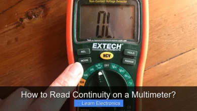
Continuity Testing
Using a multimeter, perform a continuity test on critical traces to confirm electrical connections. Check continuity between points that should be connected and ensure there is no continuity between points that should be isolated. This is particularly important for power and ground planes, as well as complex signal paths. For double-sided boards, verify connections between vias as well. This practical approach confirms the integrity of your hard work.
Making your own PCB board is an empowering skill for any electronics enthusiast. While it demands precision and patience, the satisfaction of holding a custom circuit board that you’ve crafted from scratch is immense. By following these detailed steps, you can successfully navigate the process, from initial design to a fully functional prototype. Happy circuit building!
Frequently Asked Questions
What is a PCB board and why is it crucial in electronics?
A Printed Circuit Board (PCB) board is a fundamental component that mechanically supports and electrically connects electronic components using conductive pads, tracks, and features etched from copper sheets. It provides a robust and organized platform for circuits, enabling the compact and reliable assembly of electronic devices.
What essential materials and tools do I need to make a PCB board at home?
To make a PCB board at home, you’ll typically need copper-clad laminate, a resist method (like toner transfer paper or photoresist film), etchant (e.g., ferric chloride or ammonium persulfate), and safety gear. Basic tools include a laser printer for toner transfer, a drill for component holes, and an iron or UV light source depending on your resist method.
What are the fundamental steps involved in making a PCB board from scratch?
The process of making a PCB board typically involves designing the circuit layout, transferring this design onto a copper-clad board using a resist method, and then etching away unwanted copper with a chemical etchant. After etching, you’ll drill holes for components, clean the board, and optionally apply a solder mask and silkscreen.
How do I design the layout for my PCB board?
Designing a PCB board layout involves creating a schematic and then arranging components and routing traces to connect them on the board. You can use specialized Electronic Design Automation (EDA) software like KiCad, Eagle, or Altium Designer for this. These tools help ensure proper connectivity, component spacing, and signal integrity for your PCB.
What are common methods for etching a homemade PCB board?
The most common methods for etching a homemade PCB board involve using a chemical etchant to remove the unprotected copper. Ferric chloride and ammonium persulfate are popular choices, reacting with the exposed copper while leaving the resist-protected traces intact. Always follow safety precautions and ventilation guidelines when working with these chemicals.
Are there alternatives to making a PCB board myself, especially for complex designs?
Yes, for more complex or professional-quality PCB boards, it’s highly recommended to use a professional PCB fabrication service. These services offer precise manufacturing, multi-layer boards, soldermask, silkscreen, and often lower costs for larger batches, saving you time and effort compared to DIY methods.
As an Amazon Associate, I earn commission from qualifying purchases.