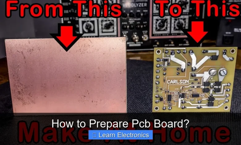
How to Prepare PCB Board? Preparing a Printed Circuit Board (PCB) board involves a series of critical steps, from initial design and material selection to fabrication data generation and quality control, ensuring the final product meets functional and reliability requirements. This comprehensive approach is essential for any electronic project, laying the groundwork for successful circuit operation.
Mastering this intricate process is fundamental for engineers and hobbyists alike, as it directly impacts the performance, longevity, and manufacturability of electronic devices. Effective PCB preparation significantly reduces development time and costs by preventing errors early in the design and production cycle.
Quick Answers to Common Questions
What’s the very first step to prepare a PCB board?
Before anything else, you need a finalized circuit design! This design will then be transferred onto your copper-clad board, typically through methods like toner transfer or photo-etching, getting you ready to prepare your PCB board for etching.
Do I need a bunch of fancy tools to get started?
Not necessarily a “bunch,” but some essentials include a copper-clad board, an etchant solution (like ferric chloride), and crucial safety gear. Basic tools like a drill, some fine sandpaper, and a container for etching will also be very helpful when you prepare your PCB board.
How can I make sure my traces come out perfectly sharp?
For crisp traces, ensure your design transfer method is precise and that your copper board is thoroughly cleaned and degreased beforehand. Agitate the etchant solution gently and uniformly to help achieve clean, sharp lines as you prepare your PCB board.
📑 Table of Contents
Understanding the PCB Design Phase
The journey of any successful electronic device begins with a robust PCB design. This initial phase dictates the functionality, physical layout, and overall performance of the circuit board.
Schematic Capture and Component Selection
The first step in this method involves creating a schematic, which is a diagram representing the electrical connections and components of the circuit. This includes selecting appropriate components based on their electrical characteristics, package types, and availability. Careful consideration of component datasheets is crucial here to ensure compatibility and performance. Using standard symbols and clear annotations makes the schematic readable and easy to debug.
PCB Layout and Routing
Once the schematic is finalized, the next step is the PCB layout. This translates the electrical connections into physical traces on the board. Key considerations include:
- Component Placement: Arranging components to optimize signal integrity, thermal management, and manufacturability. High-speed signals should be kept short, and power components need sufficient cooling.
- Trace Routing: Drawing the copper traces that connect component pads. Differential pairs, impedance control, and power distribution networks (PDN) are vital for signal integrity. Avoiding sharp 90-degree bends and ensuring adequate trace widths for current handling are common practices.
- Layer Stack-up: Determining the number of layers and their arrangement (signal, ground, power planes) to manage noise, impedance, and crosstalk.
- Design Rule Checks (DRC): Running automated checks to ensure the layout adheres to manufacturing constraints (e.g., minimum trace width, spacing, drill hole size) and electrical rules.
Material Selection and Board Sizing
Choosing the right materials and determining the physical dimensions are crucial aspects that impact the PCB’s performance, cost, and durability.
Substrate Material Considerations
The substrate, or base material, provides mechanical support and electrical insulation. The most common material is FR-4 (Flame Retardant type 4), a glass-reinforced epoxy laminate. However, specialized applications may require different materials:
- High-Frequency Applications: Materials like Rogers (PTFE-based) offer lower dielectric loss, crucial for RF and microwave circuits.
- High-Temperature Applications: Polyimide-based materials provide better thermal stability.
- Flexible PCBs: Polyimide or other flexible dielectric films allow the board to bend and conform to specific shapes.
Factors such as dielectric constant (Er), dissipation factor (Df), thermal conductivity, and glass transition temperature (Tg) must be carefully evaluated based on the application’s requirements.
Copper Weight and Thickness
The copper layers carry electrical current. Standard copper foil thickness for outer layers is typically 1 oz/ft² (35 µm) or 2 oz/ft² (70 µm). Higher current applications may require heavier copper (e.g., 3 oz/ft² or more) to prevent overheating and ensure adequate power delivery. Inner layers often use thinner copper to facilitate denser routing.
Board Dimensions and Panelization
The physical size and shape of the board are determined by the enclosure, available space, and component count. For cost-effective manufacturing, multiple identical or different PCBs are often grouped together on a larger panel, a practice known as panelization. This maximizes the use of manufacturing space and reduces per-board costs. Defining clear board outlines, cutouts, and mounting holes is part of this stage.
Preparing for Fabrication: Essential Steps for Your PCB Board
Once the design is complete, the next critical phase involves generating all the necessary manufacturing data. This practice ensures that the design can be accurately translated into a physical board by the fabricator.
Generating Gerber Files (RS-274X)
Gerber files are the industry standard for transmitting PCB design information to manufacturers. Each layer of the PCB (copper traces, solder mask, silkscreen, paste mask) is represented by a separate Gerber file. It’s crucial to generate these files correctly, ensuring they match your design intent and are compatible with the fabricator’s equipment. A typical set of Gerber files includes:
- Top Copper Layer
- Bottom Copper Layer
- Inner Copper Layers (if multi-layer)
- Top Solder Mask
- Bottom Solder Mask
- Top Silkscreen
- Bottom Silkscreen
- Solder Paste Mask (for stencil fabrication)
Excellon Drill Files
Alongside Gerber files, drill files (often in Excellon format) specify the location and size of all holes on the PCB, including through-holes, vias, and mounting holes. These files are crucial for the drilling process. It’s important to verify that the drill files accurately reflect the drill sizes specified in your design rules.
Bill of Materials (BOM) and Assembly Drawing
While not strictly part of the PCB fabrication, a comprehensive Bill of Materials (BOM) and an assembly drawing are essential for the subsequent assembly process. The BOM lists all components, their quantities, part numbers, and manufacturers. The assembly drawing provides visual instructions on component placement and orientation. These documents are often submitted alongside the fabrication data for a complete manufacturing package.
Here’s a table summarizing common PCB fabrication data files:
| File Type | Purpose | Typical Extension |
|---|---|---|
| Gerber (RS-274X) | Copper layers, solder mask, silkscreen, paste mask | .GTL, .GBL, .GTS, .GBS, .GTO, .GBO |
| Excellon Drill File | Drill hole locations and sizes | .TXT, .DRL, .XLN |
| Netlist | Electrical connectivity information | .IPC, .NET |
| Fabrication Drawing | Mechanical dimensions, stack-up, special instructions | .PDF, .DWG |
PCB Fabrication Process Overview
With all the design and data preparation complete, the actual manufacturing of the bare board can begin. This intricate process involves multiple stages that transform raw materials into a functional circuit board.
Imaging and Etching
The process starts by applying a photosensitive resist to the copper-clad laminate. The design pattern for each layer is then transferred onto the resist using UV light. After exposure, the resist is developed, leaving behind the desired copper pattern protected, while the unwanted copper is etched away chemically. This technique is repeated for each copper layer.
Drilling and Plating
Once the copper patterns are defined, holes are drilled through the board according to the Excellon drill files. These holes serve various purposes: component leads, vias for inter-layer connections, and mounting holes. After drilling, a thin layer of copper is chemically deposited into the holes (electroless plating) to make them conductive. Subsequent electroplating thickens this copper, creating robust connections between layers.
Solder Mask and Silkscreen Application
A solder mask, typically a green epoxy-based polymer, is applied over the entire board surface, except for the component pads and other areas intended for soldering. This protective layer prevents solder bridges and protects the copper traces from environmental factors. Finally, the silkscreen layer, which includes component designators, logos, and polarity indicators, is printed onto the board using non-conductive ink. This aids in assembly and troubleshooting.
Optimizing Your PCB Board Preparation Process
Beyond the technical steps, adopting best practices and understanding common pitfalls can significantly enhance the success rate of your PCB projects.
Design for Manufacturability (DFM) Principles
Integrating DFM considerations early in the design phase is paramount. This involves designing the PCB in a way that simplifies and optimizes the manufacturing process, reducing costs and potential errors. Key DFM aspects include:
- Standardized Features: Using standard trace widths, clearances, and drill sizes whenever possible.
- Component Spacing: Ensuring adequate spacing between components for automated pick-and-place machines and rework.
- Test Points: Incorporating dedicated test points for easier debugging and functional testing.
- Panelization: Designing the board so it can be efficiently panelized for volume manufacturing.
Version Control and Documentation
Maintaining rigorous version control for all design files (schematics, layouts, Gerber files, BOMs) is crucial. This ensures that you can track changes, revert to previous versions if needed, and communicate effectively with manufacturers. Comprehensive documentation, including fabrication notes, assembly instructions, and any special requirements, prevents misunderstandings and costly delays.
Communication with Fabricators and Assemblers
Effective communication with your PCB fabricator and assembler is vital. Before finalizing your design, consider consulting with them about their capabilities and preferred file formats. Providing clear, unambiguous instructions and responding promptly to any queries can prevent manufacturing issues and ensure a smooth production flow. A well-prepared data package and open dialogue are key to a successful outcome.
Conclusion
How to Prepare PCB Board? The preparation of a PCB board is a multi-faceted process demanding precision, foresight, and adherence to industry best practices. From the initial conceptualization and schematic design to the meticulous layout, material selection, and generation of manufacturing data, each step plays a crucial role in the creation of a reliable and high-performing electronic circuit. Mastering this intricate process not only ensures the functional success of your electronics but also optimizes manufacturing efficiency and cost-effectiveness. By carefully following these guidelines and maintaining clear communication with your manufacturing partners, you can confidently transform your electronic visions into tangible, operational hardware, securing the foundation for innovation and progress in the world of electronics.
Frequently Asked Questions
What are the fundamental steps involved in preparing a PCB board?
The process typically starts with transferring your circuit design onto a copper-clad board using methods like toner transfer or photoresist. This is followed by etching, which removes unwanted copper, and then drilling holes for components. Finally, you might clean, tin, or apply a solder mask to the prepared PCB for protection.
What materials and tools are essential for DIY PCB preparation?
You will primarily need a copper-clad board, an etchant (such as ferric chloride or ammonium persulfate), and a way to transfer your design like a laser printer for toner transfer or a UV exposure unit for photoresist. Essential tools include a drill for component holes, safety gear, and basic cleaning supplies like steel wool and acetone.
How do I effectively transfer my circuit design onto the PCB board?
The most common DIY methods are toner transfer and photoresist. For toner transfer, print your design onto special paper using a laser printer and then iron it onto the copper-clad PCB, ensuring the toner adheres. The photoresist method involves applying a photosensitive film to the board, exposing it to UV light through a printed transparency, and then developing it to reveal your circuit.
What safety precautions are important when preparing a PCB board at home?
Always wear appropriate personal protective equipment, including chemical-resistant gloves and eye protection, especially when handling etchants. Ensure you work in a well-ventilated area to avoid inhaling chemical fumes. Properly dispose of used chemicals according to local regulations, as they can be hazardous to the environment.
As an Amazon Associate, I earn commission from qualifying purchases.